Optical Communications and Microwave Laboratory
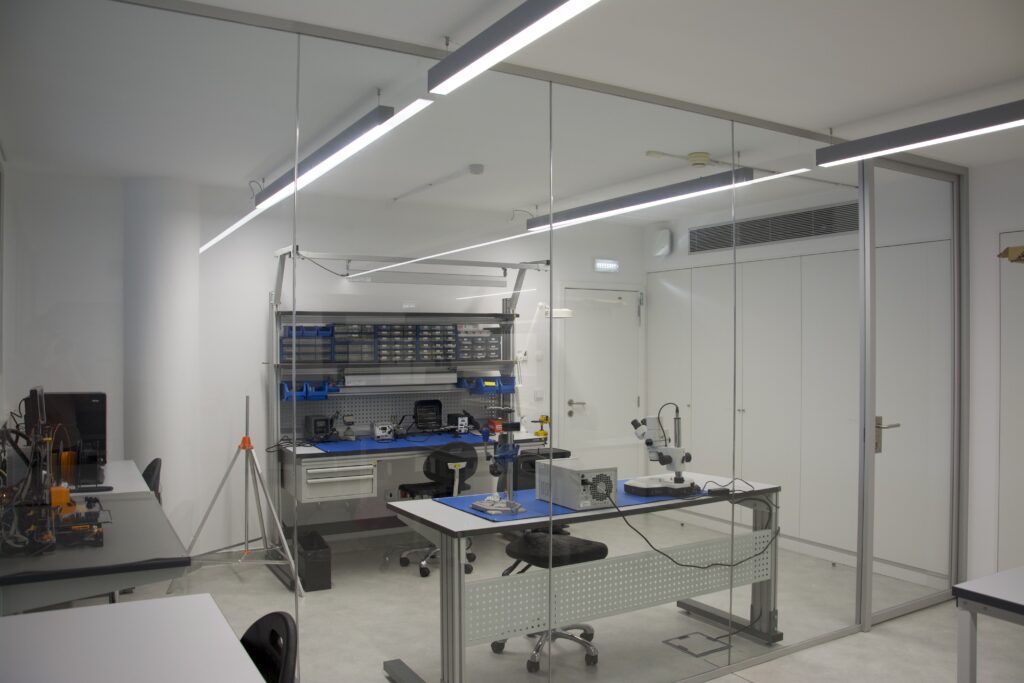
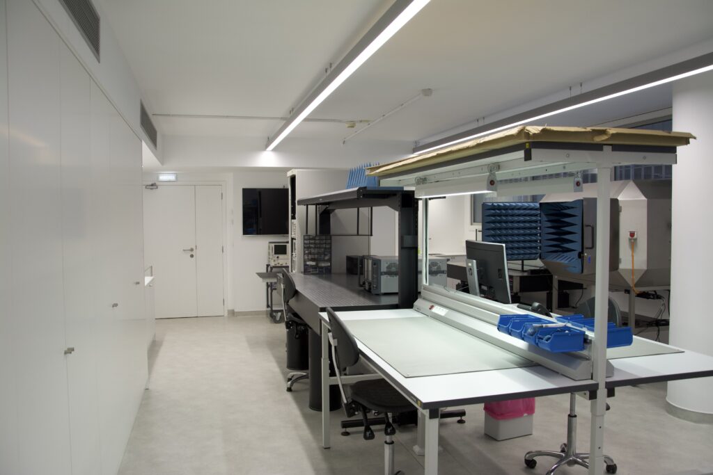
The Optical Communications and Microwave Laboratory is an Advanced World Class laboratory for optical and microwave communications, located at INESC TEC’s main building, that supports different research activities.
The laboratory was created in 2006 by Professor Henrique Salgado and is used by collaborators, working at CTM, for R&D purposes. The expansion of the laboratory was funded by the Foundation for Science and Technology (FCT) under the National Program for Scientific Hardware Renewal (PNRC) with the aim of renewing the national scientific infrastructure, by financing the acquisition, updating, and expansion of scientific equipment.
More recently, in 2021, the laboratory underwent a total refurbishment having now not only excellent conditions for researchers but also better conditions for carrying out the experiments.
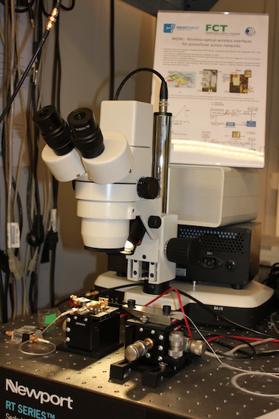
Notable equipment:
• Pattern Generator and Error Detector (Serial BERT), Agilent N4901B-100, 13.6 Gbit/s;
• PSG Analog Signal Generator, Agilent E8257D, 40 GHz;
• Arbitrary Waveform Generator, Keysight M8190A, 12-bit resolution up to 12 Gas/s;
• Lightwave Component Analyzer, Agilent E8703B, 20 GHz, 1550 nm optical modulator/ photodetector;
• Vector Network Analyzer, Agilent E8363B, 40 GHz;
• Precision Network Analyzer, Keysight N5224B, 43.5 GHz;
• FieldFox Handheld RF Analyzer, Keysight N9914A, 6.5 GHz;
• Frequency Extension Module, Keysight N5262BW10, 75 GHz – 110 GHz;
• Oscilloscope Mainframe, Agilent 86100C, with 53 GHz Optical / 63 GHz electrical module;
• Infiniium High Performance Oscilloscope, Agilent 90604A, 6 GHz, 40 GSa/s;
• Digital Storage Oscilloscope, Keysight DSOX2022A, 200 MHz, 2 GSa/s;
• PXA Spectrum Analyzer, Keysight N9030A, 50 GHz;
• Optical Spectrum Analyzer, ANDO AQ6317B, 600 nm to 1750 nm with a 0.1 nm resolution;
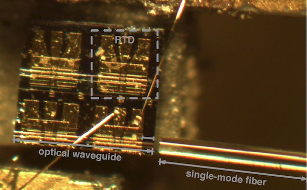
• Others: Laser diode controller, Mach-Zehnder Modulator 12 GHz with driver, Electro-Absorption Modulators 40 GHz/60 GHz with driver, Direct Modulation Laser 12 GHz with TEC controller, Bench-top EDFA, Optical Attenuator MM/SM, Tunable Laser 1510 nm-1590 nm, Optical Polarization Controllers, Time Interval Analyzer/Counter with 8 ps resolution, Optical/RF Splitters, and circulators.
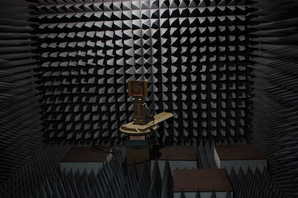
The laboratory also affords a 1.2 m x 0.6 m x 0.6 m electrically large anechoic chamber designed for evaluating different source antennas on mm-wave bands. The radio wave absorbers used offer a guaranteed reflectivity for a perpendicularly incident plane wave in the frequency range from 40 GHz to 110 GHz.
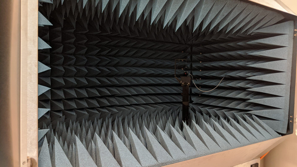
Anechoic Chamber
The anechoic chamber, located at FEUP facilities, is used to characterize RF devices, such as antennas, feedhorns, and antenna arrays. The chamber includes a vectorial network analyzer and antenna positioner, suitable for automatic measurement routines. Antenna radiation patterns can be automatically determined, in both azimuth and elevation (for both E and H planes).